
With high-resistivity silicon wafers, Chinese solar panels achieve record efficiency and will exceed 584 TWh of production in 2024.
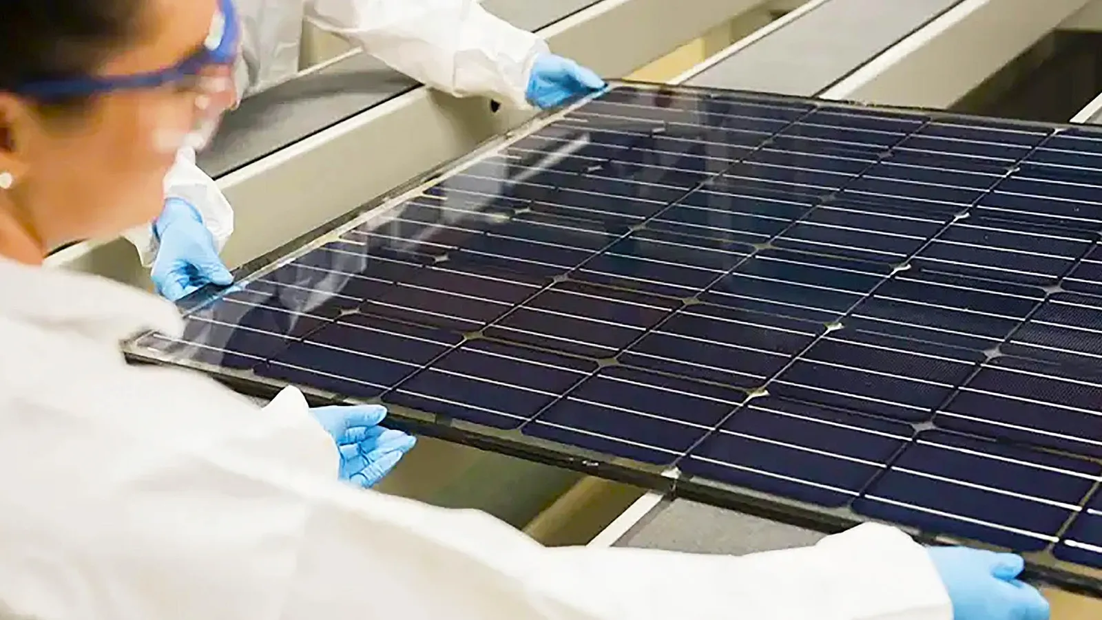
The race to improve solar energy efficiency has seen a new breakthrough led by China. Researchers and manufacturers in this Asian country have managed to enhance the performance of photovoltaic cells through a key optimization in silicon wafer treatment.
This development could help increase electricity production without the need to expand installed capacity.
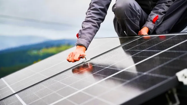
The global landscape of photovoltaic energy
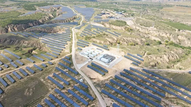
This research comes at a time of rapid global expansion in solar energy, with China playing a dominant role in this sector. According to 2024 data from DPV Energy, the country generated 584 TWh of electricity from photovoltaic solar power, the highest figure in the world. Far behind are the United States at 238 TWh, India at 113 TWh, and Japan at 110 TWh.
In Europe, Germany remains the leader with 62 TWh, despite having lower solar radiation levels than countries in the southern part of the continent. Its leadership is attributed to years of sustained support policies, such as subsidies, tax incentives, and favorable regulated rates for self-consumption and renewable energy generation.
The contrast is evident in the case of Spain, one of the sunniest countries in the world, with over 300 sunny days per year and between 2,500 and 3,000 hours of solar radiation, yet it has not yet fully utilized its photovoltaic potential.
New high-resistivity silicon wafers
Amid this landscape of growth and technological competition, one of the most influential companies is LONGi Green Energy Technology, founded in 2000 and regarded as the world’s largest manufacturer of monocrystalline silicon products—the most efficient technology in the solar industry today. The company operates across five main areas, including the production of wafers, cells, and photovoltaic modules, such as the well-known Hi-MO series panels used in both residential homes and large-scale solar plants.
The latest advancement by LONGi, developed in collaboration with researchers from Sun Yat-sen University, focuses on improving the performance of high-resistivity silicon wafers. This type of material offers theoretical advantages in terms of efficiency over standard wafers produced using the Czochralski method, which have moderate or low resistivity, greater mechanical strength, and better tolerance to thermal stresses. These properties facilitate their industrial processing and reduce the risk of damage during manufacturing.
However, initial tests revealed a problem: high-resistivity wafers tended to exhibit performance below expectations. Analysis showed they operated with higher densities of excess carriers at the maximum power point and flatter concentration gradients. This behavior reduced carrier accumulation and increased their sensitivity to recombination at the edges.
In practice, without specific treatment, the wafer edges acted as a load loss point, negating the theoretical advantages of the material.
The solution proposed by the team has been edge passivation, a process that reduces those losses and allows control over recombination. The researchers found that the combination of high resistivity and effective passivation is key to achieving maximum performance, as these wafers more easily enter the high-level injection regime—a physical characteristic that favors higher fill factors and, thus, greater efficiency.
Thanks to this control, the wafers can maintain more efficient carrier collection and turn their theoretical potential into superior real-world performance.
To validate the process, the team manufactured hybrid back-contact interdigitated (HIBC) solar cells with dimensions of 18.3 centimeters by 9.1 centimeters, using both high-resistivity wafers and standard Czochralski wafers. The main difference in the experiment was that, for the high-resistivity wafers, the edges were left without silicon nitride during vapor-phase chemical deposition, leaving the SiOx/n-poly-Si passivation layer exposed and partially removed during wet chemical cleaning.
The entire manufacturing process involved several industrial stages: wet chemical cleaning, chemical vapor deposition (CVD), phosphorus diffusion, atomic layer deposition (ALD), laser patterning, physical vapor deposition (PVD), electrical insulation, and screen printing.
Subsequently, the cells were analyzed using IV curve testers, wafer metrology systems, transmission electron microscopy, and simulation tools.
The results confirmed the impact of the treatment: the incorporation of effective edge passivation improved performance in both low- and high-resistivity cells, although the gains were significantly greater in the latter.
This technical advancement, though with industrial implications, reinforces the industry’s trend toward incremental improvements in silicon—a material that remains the basis for over 90% of the world’s solar panels. In a market where even small increases in efficiency reduce costs and boost output per square meter, developments like this solidify China’s technological leadership and bring us closer to a scenario where energy
