
Infineon processes SiC on 300 mm wafers for the first time
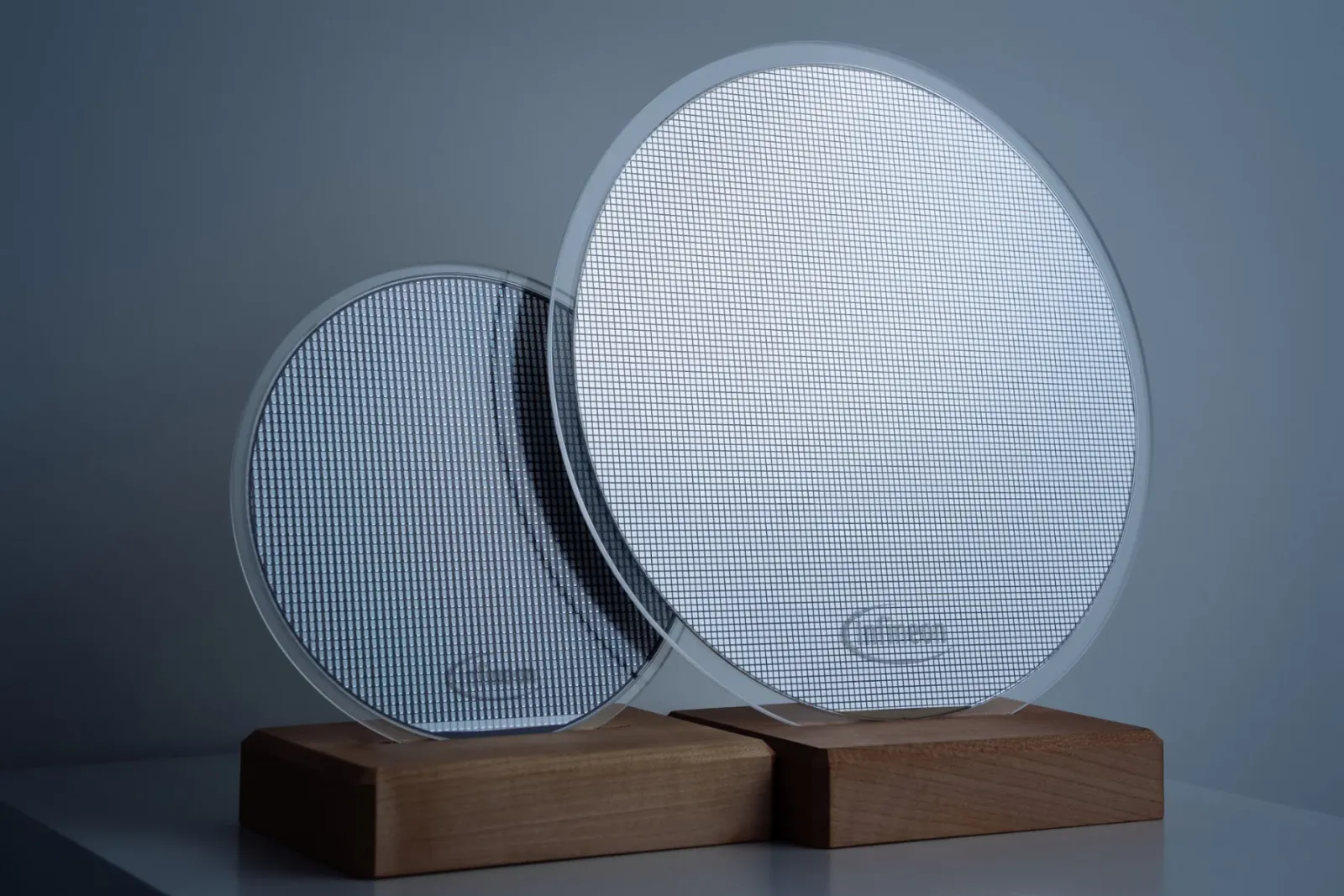
Infineon has produced the first functional SiC power devices on 300-millimeter wafers. The larger wafer diameter is intended to make production more efficient and, in the long term, improve supply for applications including EVs and charging infrastructure.
300 mm SiC wafer enables 2.3 times more chips than 200 mm.
Image: Infineon
The semiconductor manufacturer has, for the first time, processed 300 millimetre silicon carbide (SiC) wafers under real production conditions at its plant in Villach, Austria. According to the company, Infineon is the first to achieve this milestone in semiconductor manufacturing. Existing production facilities were used, which can also process silicon.
The key advantage of the larger wafers lies in improved yield: a 300 mm wafer enables approximately 2.3 times as many chips as a 200 mm wafer, according to Infineon. This allows for more efficient scaling of production in the future. However, Infineon has not yet specified a concrete timeline for ramping up production. The company intends to determine this in collaboration with customers and partners. At the same time, the existing roadmap for 200 mm SiC production will continue to be implemented.
Silicon carbide is currently one of the most important wide-bandgap materials for power electronics. Compared to conventional silicon, SiC enables lower power losses, higher power densities, and efficient operation at high voltages and temperatures. Applications include traction inverters, on-board chargers, and charging stations for electric vehicles, as well as stationary storage systems and industrial drives.
SiC remains critical for e-mobility and charging infrastructure
For electromobility, this step is particularly relevant in terms of scaling and manufacturing costs. Larger wafers can produce more SiC chips per production run, potentially enabling cost-effective production of larger quantities in the long term. However, Infineon has not made any specific statements regarding possible cost reductions for individual components.
In parallel, the company is also working on more efficient production of the SiC wafers themselves. At its Dresden site, Infineon has successfully tested the so-called cold-split technology for 300 mm SiC. This method separates wafers from a SiC crystal with less material loss and shorter processing times compared to conventional wire sawing. As a result, more wafers can be obtained from the same crystal.
This SiC milestone builds on Infineon’s 300 mm strategy in Villach. There, the company had already prepared the transition from 200 to 300 mm wafers for gallium nitride and announced at the end of October that it would invest around €1.1 billion euros in the site by 2034. High-volume production of GaN power semiconductors on 300 mm wafers is scheduled to begin at the end of 2027.
With SiC, Infineon is now transferring this manufacturing approach to a second wide-bandgap material. The company thus produces power semiconductors based on silicon, gallium nitride, and silicon carbide, and relies on 300 mm technology for all three materials.