
A closer look at GaN switches: benefits, limitations and gate-drive challenges
EV Engineering News
Posted October 28, 2026 by Jeffrey Jenkins & filed under Features, Newswire, Tech Features, The Tech.
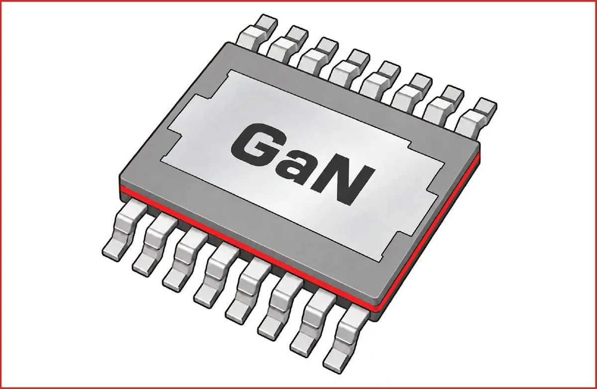
Switches based on the wide band-gap semiconductors SiC (silicon carbide) and GaN (gallium nitride) have been gaining market share on their conventional silicon counterparts over the last decade or so because they deliver lower total losses at higher switching frequencies and power levels, all at an increasingly competitive price. SiC MOSFETs are far more popular than GaN (MOS)FETs, however, and the parenthetical aside, “(MOS)FETs,” is the first clue why: GaN switches can be constructed in numerous ways, with differing behaviors between them.
GaN does have its advantages, and in some applications, it is no hyperbole to call it a game-changer.
In contrast, SiC MOSFETs behave more or less the same as their conventional Si counterparts, and often come in the same standardized packages, so it’s entirely possible to get decent-enough results by merely substituting SiC for Si in an existing design (though getting optimal results will take some effort, so don’t be too lazy!).
SiC also has a much higher thermal conductivity and can operate at much higher junction temperatures than either GaN or Si—two advantages which are especially attractive in EV/hybrid applications. In an article that is ostensibly about GaN, this is sounding more like a sales pitch for SiC, but GaN does have its advantages, and in some applications, it is no hyperbole to call it a game-changer.
The goal behind the development of wide band-gap semiconductors is, somewhat paradoxically, to get them as close as possible to being an insulator without actually becoming one, because this reduces the physical size of the die for a given voltage and current rating. The latter might seem unbelievable, but there are three synergistic factors at work here: the first is that breakdown voltage in a material is a linear function of the distance between opposing polarities (e.g. the drain and source terminals), and of its critical field specification (typically given in MV / cm), while the critical field is an exponential function of its band-gap energy. The upshot is that the critical field for SiC is approximately 10x higher than that of Si, while for GaN it is closer to 14x higher, meaning that device geometries can be that much smaller for a given breakdown voltage.
The second factor is that the on resistance goes up with the square of breakdown voltage, but goes down with the cube of critical field, which effectively means that on resistance is a linear function of breakdown voltage (among other factors) for a given material, but inversely proportional to the cube of the critical field value for different materials; ergo, on resistance is 143 lower in GaN right there! The mobility of charge carriers (i.e. electrons in an n-type material; holes in a p-type) also influences on resistance (and switching speed, more obviously), and GaN excels here, too, with an electron mobility ranging from 1,500 to 2,000 (in units of cm2 / s), compared to ~1,400 for Si and ~950 for SiC. GaN ought to be running circles around SiC, then, when it comes to on resistance vs breakdown voltage—not to mention its blistering high speed, by virtue of its electron mobility—yet the GaN switches that are actually in stock at Mouser, for example, top out at 650 V, whereas there are hundreds of different SiC part numbers rated for 1,200 V or higher. There may be all sorts of reasons why, but I suspect this is more of a tacit acknowledgment that no one really wants to switch 800 V (or more!) in 10 ns (or less!).
In its most basic structure, a GaN switch typically consists of a lateral n-GaN drain-source channel with an AlGaN barrier layer on top to separate it from the gate (the gate itself may take on several forms). Strain between the interface of the n-GaN and AlGaN layers creates a sheet of electrons—colorfully referred to as a two-dimensional electron gas, or 2DEG—which results in the drain-source channel being highly conductive by default (aka depletion-mode operation). Normally-on switches are a bit of a hazard in most power converter circuits, but it is possible to convert GaN over to normally-off (enhancement-mode) operation via modifications to the gate structure, or with an additional MOSFET, wired either in cascode (giving true enhancement-mode operation), or in series with the source terminal of the GaN switch (acting more as a static “safety” switch). The existence of all these different schemes explains why GaN switches from different manufacturers and/or device generations can behave differently, and have subtly (or vastly) different gate drive requirements.
GaN can typically withstand a surprising amount of overvoltage without avalanching (though at a high enough overvoltage it will avalanche, and not gracefully, either).
GaN has some other quirks, but a particularly unusual (though not unwelcome) one is that it can typically withstand a surprising amount of overvoltage without avalanching (though at a high enough overvoltage it will avalanche, and not gracefully, either). That’s not an invitation to exceed the VDS rating given on the datasheet, but it does imply that one need not be as conservative with voltage derating GaN as with other switch types. On the flip side, GaN tends to have a very anemic pulse current rating, exhibiting a phenomenon called current collapse (similar to desaturation in an IGBT) in which the device basically runs out of gain, causing the drain-source voltage to soar above a certain current, hence one should be rather generous with the current derating. For example, the datasheets of two switches from Infineon, the IGK048B041S GaN FET and the BSC059N04LS6 Si MOSFET, which have similar voltage, continuous current and on resistance ratings, claim a pulsed current rating of 120 A for the GaN switch and 263 A for the Si one (neither is realistically achievable, of course, but the relative comparison is nonetheless telling). The quirkiest quirk is that a conventional enhancement-mode GaN switch (i.e. not with a cascode or series MOSFET) exhibits zero recovery time during reverse conduction, but with a source-drain voltage drop that is the sum of its gate threshold voltage and any negative bias voltage applied to the gate. An example of where this can be an issue is during the deadtime between the switches in a half-bridge (see below on gate drivers), but a simple solution is an external fast-recovery or Schottky diode in anti-parallel. The drain-source channel will take up reverse conduction initially, but its relatively large voltage drop will slew the current through any stray inductance over to the external diode in short order.
The real reasons for considering GaN in the first place are its blazing fast switching speed and its reputation for having lower parasitic capacitances, and therefore much lower switching losses.
Of course, the real reasons for considering GaN in the first place are its blazing fast switching speed and its reputation for having lower parasitic capacitances, and therefore much lower switching losses, but beware that the latter may only be true at higher voltages. For example, the capacitances and gate charge values are roughly the same in the aforementioned 40 V switches, but comparing two similarly rated parts from Infineon at the 650 V level shows a clear advantage for GaN: input capacitance is ~7x lower and total gate charge is ~12x lower in the GaN IGLD65R140D2AUMA1 vs the Si IPL65R195C7AUMA1.
To actually make use of GaN’s extreme speed—and to realize its promise of lower switching losses—requires even more care than usual in minimizing loop inductances, especially in series with the source terminal, the local bypass capacitor(s), and the gate, as even 1 nH of stray inductance in these loops can cause real headaches with ringing and overshoot at the 1-10 ns switching speeds possible with GaN. This is also why packages that are rarely used elsewhere for power devices (e.g. BGA and LGA) are so common in GaN, on the premise that their demonstrably lower stray inductances outweigh their relatively higher fragility (vis-a-vis temperature swings, vibration and impact), costlier PCB construction, and even more costly x-ray inspection for verifying solder joint integrity.
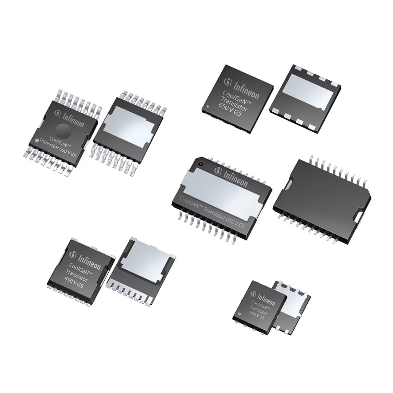

As mentioned above, the different approaches to enabling enhancement-mode behavior in GaN switches have resulted in a diverse range of gate drive requirements. For example, the construction using a cascode MOSFET inherits its behavior, meaning that the overall GaN switch is off at 0 V, fully on at +10 V, and will tolerate a maximum of +/- 20 V, while the construction using a series MOSFET really just uses the latter to block conduction in the GaN switch by default. Among the modified gate structure constructions there is less variability in behavior, but in all cases there is a rather narrow margin between the threshold (+1 to +2 V), fully enhanced (+4 to +5 V) and maximum allowed voltages (+6 V, typical).
Also note that some GaN constructions require no gate current to maintain conduction (i.e. behave like MOSFETs), while some will require a few mA to 10s of mA of forward bias, which may also be proportional to drain current (like a BJT!). One subtle factor which emerges from the above is that the relatively low threshold voltage does lower total gate charge, but also results in a much higher susceptibility to spurious turn-on as a result of ringing on the gate, commutation of the opposite leg switch in a half-bridge, etc. However, the usual solution of biasing the gate with a negative voltage when off works well here, and there is somewhat more flexibility in that anything from -1 V to -10 V should be fine (yes, the maximum allowed negative gate voltage can [sometimes] be higher than the positive). There is no upside to the paltry gap between optimum and maximum gate voltages, however, and this is why GaN needs “more than usual care” with its gate drive. Towards that end, the four options are:
Use a conventional gate driver (or switchmode controller) IC intended for MOSFETs or IGBTs, which will likely have too much enforced deadtime if it is a half-bridge type, while also requiring a much higher supply voltage to get out of UVLO, so you’ll need to clamp the gate voltage with a zener(s), wasting power that may be in short supply (e.g. derived from the bootstrap circuit or a small isolated DC/DC converter).
Use a GaN-specific gate driver IC with appropriate supply voltage(s).
Design a discrete voltage-limited current-source driver circuit specifically for the application.
Use a GaN switch (or half-bridge array) with integrated gate driver(s).
The first solution is very tempting, I know, but should be avoided for its overall poor performance. The second solution has the best mix of flexibility, performance and cost, followed by the third solution, which is rather less palatable due to the board area required, and the strays that come with it. Finally, the last solution is capable of the best switching performance, unsurprisingly, but at the cost of extreme susceptibility to supply chain disruption, also unsurprisingly. Otherwise, you really do need to consult the datasheet and application notes from the specific manufacturer of the specific GaN switch for the recommended gate drive conditions (and/or driver circuit/ICs), as you probably won’t get away with recycling the same basic gate drive design from one GaN application to the next, as you can do with Si (or even SiC) MOSFETs.
GaN is also just different enough from anything else that one is well-advised to do more reading than just the manufacturer-supplied app notes.
GaN has its advantages and disadvantages, but it is also just different enough from anything else that one is well-advised to do more reading than just the manufacturer-supplied app notes, and towards that end I can recommend the book GaN Power Devices for Efficient Power Conversion by Lidow et al, which is on its fourth edition (2025). Otherwise, GaN is very compelling whenever minimizing the volume and/or weight of reactive energy storage components from a massive increase in switching frequency is a high priority, such as an onboard charger or DC/DC converter. Conversely, GaN would be a poor fit in the traction inverter, with its relatively low pulse current capability—meaning more over-dimensioning than usual will be prudent—and its faster switching speed is not just wasted, but is actually a negative (from the higher dV / dt accompanying such). That said, technical superiority is irrelevant if you can’t get the same part number—or a drop-in substitute—a year or two from now, and GaN does seem to be uniquely susceptible to this problem with its double-whammy of being a rapidly evolving switch technology that also tends to come in unusual packages; needing a board redesign which then triggers a renewed round of safety and EMC compliance testing is nobody’s idea of a good time.
This article appeared in Issue 77: July-September 2026 – Subscribe now.
Create Account. Already Registered? Log In
Virtual Conference on EV Engineering: Free to Attend
Don't miss our next Virtual Conference on September 14-17, 2026.
Register for the free webinar sessions below to reserve your spot and watch them live or on demand.
LOAD MORE SESSIONS